SPAD Depth Sensor for Automotive LiDAR Applications

SPAD Depth Sensor for Automotive LiDAR Applications

Contributing to the future of safe and secure mobility through the evolution of automotive LiDAR detection and recognition performance

Overview

The Automotive Light Detection and Ranging(LiDAR), which can accurately detect and recognize road conditions and the positions and shapes of objects such as vehicles and pedestrians, is a technology that is becoming increasingly important for the spread of Advanced Driver Assistance Systems (ADAS) and the realization of Automated Driving.

A Single Photon Avalanche Diode(SPAD) is a pixel structure that uses “avalanche multiplication” to multiply electrons from a single incident photon, like a real world avalanche . It allows detection even when the incident light is weak. Distance measurement over long distances and with high accuracy are made possible by using this structure as the light receiving element in the SPAD ToF depth sensor. This sensor measures the distance to an object by detecting the Time of Flight (time difference )of a signal emitted from a light source until it returns to the image sensor, after being reflected by an object.

Technologies that Sony Semiconductor Solutions Corporation has nurtured in CMOS image sensor development such as the back-illuminated structure, stacked structure, and Cu-Cu (copper-copper) connection*1 have been utilized in this product, to include the SPAD pixel and distance processing circuits in a single chip, realizing high resolution in a compact size. This allows this product a highly accurate and rapid measurement of a distance of up to 300 m at 15 cm range resolutions*2. The product also contributes to improved reliability for the difficult requirements for automotive applications, such as for various temperature environments and weather, etc..The inclusion in a single chip also contributes to the reduction of costs for LiDAR.

*1) A technology used when a pixel chip (top) is stacked with a logic chip (bottom), to achieve electrical continuity by connecting the Cu (copper) pads to each other. This increases the freedom in the design, improves productivity, and enables a smaller size and higher performance compared with Through-Silicon Vias(TSV), where the upper and lower chips are connected by through electrodes around the circumference of the pixel area.

*2) When measuring an object with a height of 1 m and reflectance of 10% in cloudy daytime conditions with 6 pixels (H) x 6 pixels (V) in additive mode.
Features

High-speed, high-precision distance measuring performance thanks to a stacked configuration with both 10 μm square SPAD pixels and distance measuring processing circuit


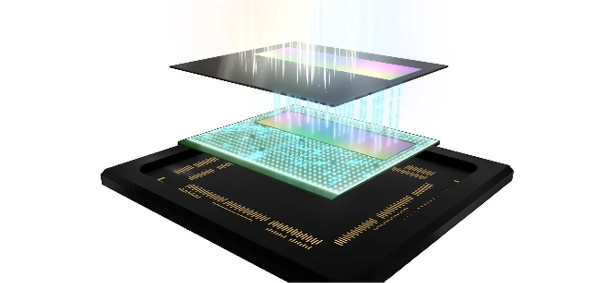
The new technology employs a back-illuminated SPAD pixel structure that uses a Cu-Cu connection, to connect each pixel in the pixel chip (top) to the logic chip equipped with distance measuring processor circuits (bottom). Because this configuration places all circuits below light receiving pixels, it allows a high aperture ratio*3 and a high 22%*4 photon detection efficiency rate. Even with its compact chip size, a high resolution of approximately 110,000 effective pixels (189 x 600 pixels) at a pixel size of 10 μm is achieved. This enables high-precision distance measuring at 15-centimeter range resolutions up to a distance of 300 meters, thereby contributing to improved LiDAR detection and recognition performance.

*3) Ratio of aperture section (section other than light-blocking sections) as viewed from the light incident side per pixel.

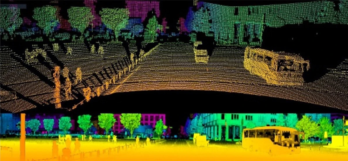
SPAD ToF depth sensor stacked configuration (Top: point cloud, bottom: distance intensity image)

Imaging example of LiDAR with SPAD ToF depth sensor (Top: SPAD pixels, bottom: distance measuring processing circuit)


Compliant with the feature safety standards for automotive applications, improving the reliability of LiDAR systems

We are planning to obtain AEC-Q100 Grade 2 certification, the standards for reliability testing of automotive electronic devices. Our development process is also compliant with ASIL-B (D) under ISO 26262, the international standards for the safety of road vehicles, dealing with feature safety aspects like failure detection, notification and control. This contributes to the improvement of the reliability of LiDAR systems.


What is direct Time of Flight (dToF)?

dToF is a measurement method that measures the distance to an object based on the Time of Flight (time difference) of a signal emitted from a light source until it returns to the image sensor, after being reflected by an object.
Depth sensors with dToF use SPAD pixels, which can detect a single photon, so they can achieve high-precision depth measurement even from a long distance.

6AAkCogpIKmfXMvsGkEiA4QUkHT8WeI1yBEAlwBhAQIWlBKon4dQOECQgIAwBlASAAAOAMICQAAZwAhAQDgDCAkAACcAYQEAIAzgJAAAHAGEBIAAM4AQgIAwBlASAAAOAMICQAAZwAhAQDgDCAkAACcAYQEAIAzgJAAAHAGEBIAAM4AQgIAwBlASAAAOAMICQAAZwAhAQDgDCAkAACcAYQEAIAzgJAAAHAGEBIAAM4AQgIAwBlASAAAOAMICQAAZwAhAQDgDCAkAACcAYQEAIAzgJAAAHAGEBIAAM4AQgIAwBlASAAAOAMICQAAZwAhAQDgDCAkAACcAYQEAIAzgJAAAHAGEBIAAM4AQgIAwBlASAAAOAMICQAAZwAhAQDgDH8FAADgCv8fUTx5Pils56cAAAAASUVORK5CYII=

The mechanism of SPAD (single photon avalanche diode) pixels

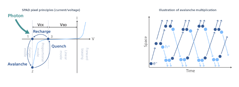
On a dToF depth sensor, SPAD pixel is able to detect single photons. Breakdown Voltage (VBD)*4 is applied to the electrodes in the SPAD pixel. By setting Excess bias Voltage (VEX)*5 exceeding VBD to the electrodes, when the pixel is hit by photons the electrons generated in photoelectric conversion are amplified via avalanche multiplication. Then, the voltage between electrodes lowers to the breakdown voltage and avalanche multiplication is stopped. After the electrons generated by avalanche multiplication are collected and the voltage has returned to the breakdown voltage (quenching action), the voltage between electrodes is set to the excess bias voltage once again to enable detection of the photon (recharge action). This multiplication of electrons triggered by the arrival of the photon is known as Geiger mode.

Sdddd.png


Technology

ToF(Time of Flight)

Find out more about ToF(Time of Flight) used in this product.

Applications

Automotive Camera/LiDAR

These products are leveraged in automotive camera/LiDAR.

back to the top